Preface:
STM32 has eight modes, as follows:
- Push-pull output
- Open-drain output
- Multiplexed push-pull output
- Multiplexed open-drain output
- Floating input
- Pull-up input
- Pull-down input
- Analog input
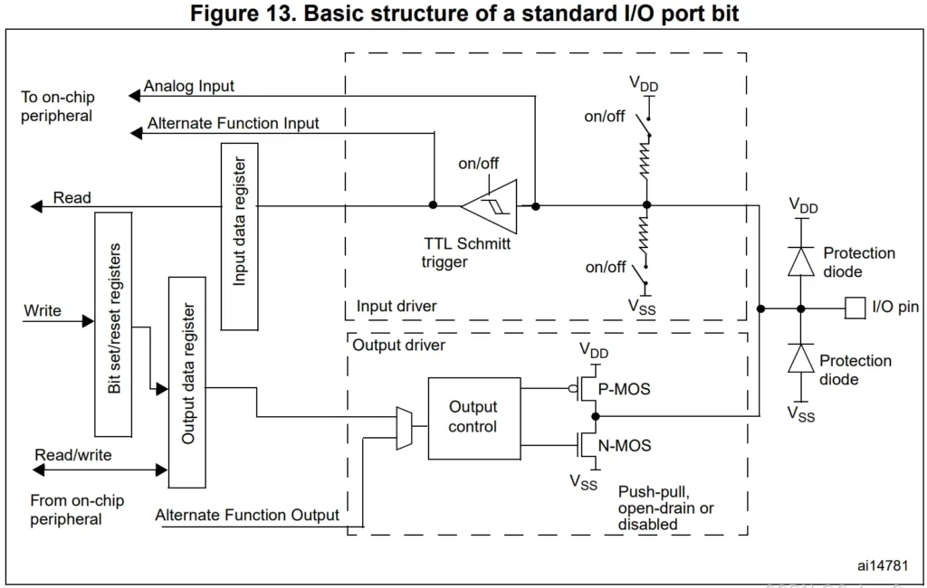
The STM32 standard IO structure diagram is as follows:
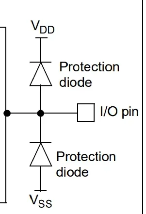
The following circuit is a protection circuit. When the voltage is greater than VDD-3.3~5V, the protection diode is turned on and the voltage is absorbed by the power supply. When the voltage is less than VSS-0V, it is absorbed by GND to protect the chip.
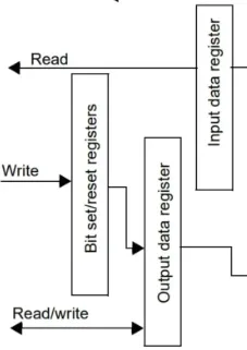
Registers are program and circuit control units. The programs we write can ultimately control circuits, mainly by switching functional circuits on and off through registers.
Similar to our commonly used HAL_GPIO_WritePin, the internal code is as follows
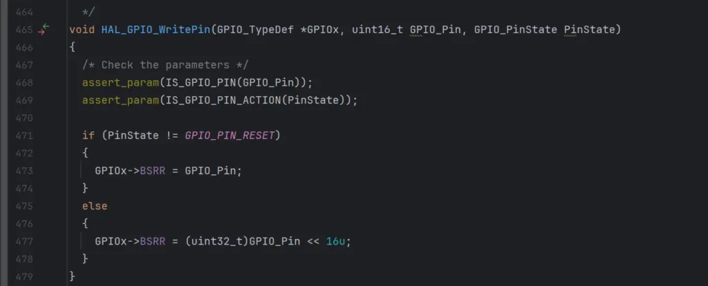
The atomic setting of GPIO pin status is mainly achieved through the BSRR register
| Operation Type | Code logic | Register behavior | Level results |
| Set (high level) | GPIOx->BSRR = GPIO_Pin | Write the pin mask to the lower 16 bits of BSRR, and set the corresponding position to 1 | Pin outputs high level |
| Reset (low level) | GPIOx->BSRR = GPIO_Pin << 16u | Write the pin mask to the upper 16 bits of BSRR, corresponding to position 1 | Pin outputs low level |
Therefore, our code mainly controls the functions of the microcontroller through the information of the control register
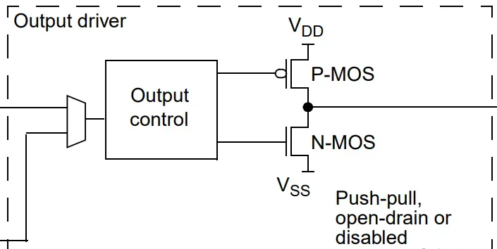
Output Driver:
The circuit diagram of the output register is as follows, which is mainly controlled by output, P-MOS and N-MOS
Universal push-pull output:
The core of push-pull output is that P-MOS and N-MOS tubes are always in complementary conduction state. When one is turned on, the other must be turned off.
The status correspondence is shown in the following table:
| Target output level | Output Control Logic | P-MOS tube status | N-MOS tube status | Current Path (Drive Strength) |
| High level (1) | Receive a set signal (such as BSRR writing 1 to the lower 16 bits) |
On (switch closed) | Cutoff (switch open) | V_DD → P-MOS → Output pin . Current flows out of the chip , actively driving the output high. |
| Low level (0) | Receive a reset signal (such as BSRR writing 1 to the upper 16 bits) |
Off (switch open) | Conduction (switch closed) | Output pin → N-MOS → V_SS (ground). Current flows from the pin into the chip, actively driving the output low. |
Universal push-pull output (Push-Pull) Features:
- Strong driving capability: Whether at high or low levels, it can actively source or sink considerable current (e.g., ±20mA), directly driving devices such as LEDs and buzzers.
- Low impedance: stable output level and strong anti-interference ability.
- Classic applications: digital signal output, driving common peripherals.
General-purpose push-pull output (GPIO_MODE_OUTPUT_PP)
- Circuit: Push-pull structure.
- Control: Direct software control.
- Applications: The most common output mode, driving LEDs, key scanning, etc.
In push-pull output mode, the small light is driven by the voltage inside the chip.
General purpose open-drain output:
General open-drain output (Open-Drain) :
- In open-drain output mode, the P-MOS transistor is completely inactive (always off), and only the N-MOS transistor is controlled. When the N-MOS transistor is off, the output pin is effectively disconnected (high impedance), requiring an external pull-up resistor to VDD to output a high level.
- Open-drain applications: Level conversion, I²C and other bus communications (can realize “wired AND” function)
General-purpose open-drain output (GPIO_MODE_OUTPUT_OD)
- Circuit: Open-drain structure.
- Control: Direct software control.
- Purpose: Software simulation of I²C protocol and ordinary IO that requires level conversion.
The open-drain output has no driving capability and must be driven by an external voltage source.
“Push-pull” and “open-drain” refer to the circuit structure that determines the electrical characteristics of the pin (how it is driven).
The biggest difference between push-pull output and open-drain output is that the push-pull output is fixed at 3.3V under high level, while the open-drain output is determined by the external circuit because the open-drain output does not control the state of the P-MOS.
Multiplexed push-pull output:
Multiplexed push-pull output (GPIO_MODE_AF_PP)
- Circuit: Push-pull structure.
- Control: Automatic control of hardware peripherals.
- Applications: SPI’s SCK/MOSI/MISO pins, USART’s TX pin, etc. These protocols require strong drive and high-speed push-pull outputs.
Multiplexed open-drain output:
Multiplexed open-drain output (GPIO_MODE_AF_OD)
- Circuit: Open-drain structure.
- Control: Automatic control of hardware peripherals.
- Purpose: SDA and SCL pins of I²C. This is required by the I²C bus standard to implement the “wired AND” function of multiple master devices.
“Universal” and “Multiplexed” refer to the source of the signal and determine who controls the pin (software or hardware peripheral)
The communication protocol used depends on the selected “multiplexing” mode and the corresponding circuit structure. For example, I²C must be configured with “multiplexed open-drain” and SPI must be configured with “multiplexed push-pull”.
Input Driver:

The input driver mainly consists of pull-up and pull-down resistors and TTL Schottky triggers
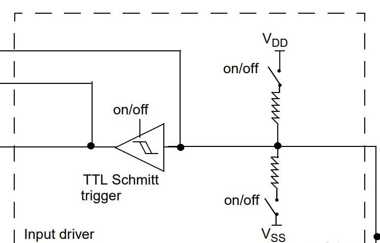
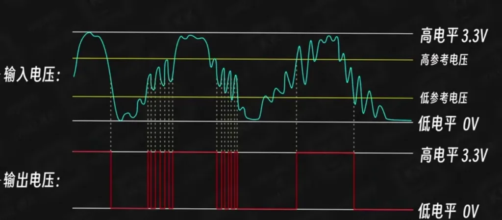
TTL Schottky trigger is mainly used to stabilize the level, because the external input voltage is not very stable and will not be stable at 3.3v and 0v to distinguish high and low levels. Therefore, the TTL Schottky trigger will generate two reference voltages, namely high reference voltage and low reference voltage. When it is higher than the high reference voltage, it outputs a high level, and lower than the ground reference voltage, it outputs a low level. The level signal does not change between the two.
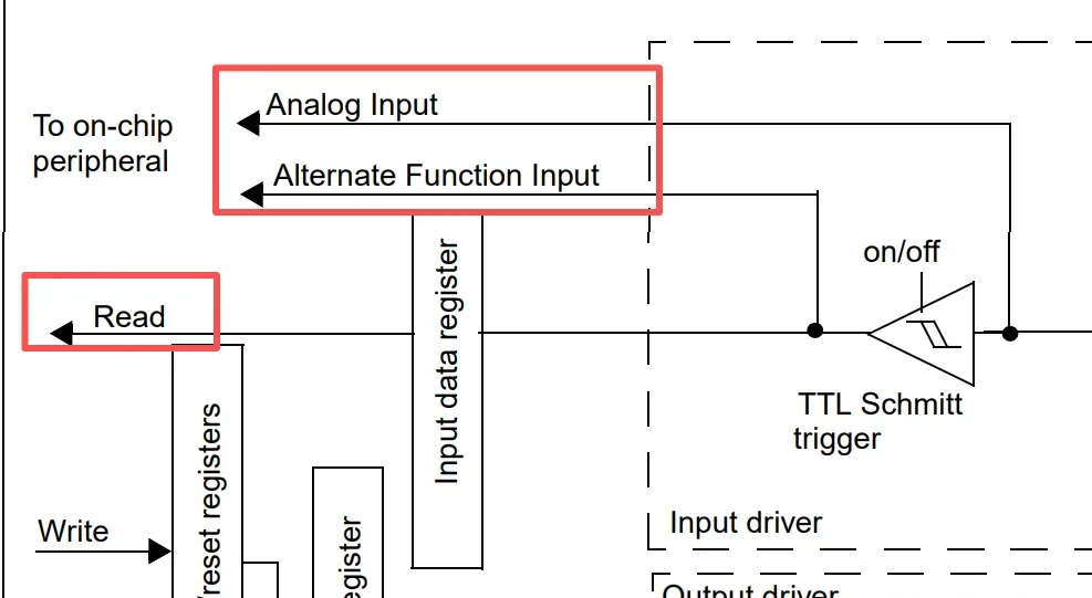
There are three branches of output, from top to bottom are analog input, multiplex function input and read
The analog input is before entering the TTL Schottky trigger, mainly to read the accurate voltage value
Floating input:
Floating input means not enabling the internal pull-up and pull-down resistors and only reading the voltage of the I/O pin
Floating Input
- Principle: The internal pull-up/pull-down resistors are completely disconnected, the pin is in a high-impedance state, and the voltage level is completely determined by the external circuit.
- Features:
- When left floating, the voltage level fluctuates randomly between 0.3–0.7VDD, which may cause logic misjudgment.
- High signal fidelity: No internal resistance interference, suitable for μV-level weak signals (such as piezoelectric sensors).
- An external driver is required: otherwise it is susceptible to static damage or noise interference.
- Application Scenarios:
- High-speed digital signal reception (UART_RX, CAN bus).
- High-precision ADC pre-stage signal acquisition (external low-impedance source required).
Pull-up input:
Pull-Up Input
- Principle: The internal resistor is connected to VDD, and the pin level is pulled high by default.
- Features:
- Default high level: reads “1” when left floating, reads “0” when externally grounded.
- Simplified circuit design: No external pull-up resistor is required (for example, the button is directly connected to ground).
- Static power consumption: About 82μA at 3.3V, so battery-powered operation requires caution.
- Application Scenarios:
- Mechanical button detection (pull down the level when the button is pressed).
- Level-holding for the I²C-bus (in conjunction with open-drain output).
Pull-down input:
Pull-Down Input
- Principle: The internal resistor is connected to GND, which pulls the pin level low by default.
- Features:
- Default low level: When left floating, the reading is “0”, and when connected to VDD externally, the reading is “1”.
- Strong resistance to power supply interference: suitable for safety monitoring (triggering high level when abnormal).
- Application Scenarios:
- Hall sensor (normal low level, magnetic trigger high level).
- DC power supply detection (the default is low level when there is no power).
Analog Input
Analog input:
- Principle: Disable digital circuits (Schmitt trigger, pull-up/down resistors) and pass the signal directly to the ADC module.
- Features:
- No digital level: The pin state cannot be read via the IDR register.
- High-precision requirements: Impedance matching is required (12-bit ADC recommends signal source impedance <1kΩ).
- Anti-interference design: An external filter capacitor/π-type filter is required to suppress noise.
- Application Scenarios:
- The ADC acquires analog signals (temperature, pressure, voltage).
- Direct sampling of sensor signals (such as thermocouples) in low power mode.
Input summary:
| characteristic | Floating input | Pull-up input | Pull-down input | Analog input |
| Internal structure | No pull-up/pull-down resistors, high impedance (>100MΩ) | Internal pull-up resistor (about 40kΩ) connected to VDD | Internal pull-down resistor (approximately 40kΩ) connected to GND | Disable digital circuits and connect directly to the ADC module |
| Default Level | Uncertain (random fluctuations when suspended) | High level (1) | Low level (0) | No digital level, only analog signal is transmitted |
| External drive requirements | An external low-impedance drive source (<10kΩ) must be connected. | Can be left floating, default high level | Can be left floating, default low level | Need to match sensor impedance (e.g. ADC needs to be <1kΩ) |
| Response speed | Extremely fast (<5ns) | Slow (about 200ns, affected by RC delay) | Slow (about 200ns) | Depends on ADC sampling rate (e.g. μs level) |
| Power consumption | Ultra-low (quiescent current ≈ 0.1μA) | High (about 82μA at 3.3V) | High (similar to pull-up) | Low (power consumption only when ADC is working) |
| Anti-interference ability | Very weak (susceptible to noise) | Stronger (default level is stable) | Stronger (default level is stable) | Depends on external filtering circuit |
| Typical application scenarios | High-speed communication (UART/CAN), high-precision sensors | Key detection, I²C bus, wake-up circuit | Light sensor, safety switch, low level trigger | ADC acquisition (temperature, pressure, voltage signals) |
Input mode selection:
- Requires high-precision analog acquisition → Analog input (e.g., ADC).
- External signals are well-defined and require a default state → Pull-up/pull-down inputs (e.g., buttons, sensors).
- High-speed or weak signal processing → Floating input + external driver (e.g., UART, precision sensor).
- Power saving scenario: Prioritize floating or analog input (lowest static power consumption)


